On August 9, 2022, President Biden passed the CHIPS Act.
What’s that? We’re here to fill you in.
The CHIPS Act
CHIPS stands for Creating Helpful Incentives to Produce Semiconductors for America Act. The investment promises $50 billion to domestic R&D and manufacturing, marking a seminal moment for US semiconductor manufacturing.
This article looks at how organizations can use the funding to create a cleanroom space that supports the semiconductor supply chain.
What does the CHIPS Act mean for OEMs?
The CHIPS Act presents an opportunity for semiconductor R&D companies and manufacturers—along with their supply chain—to upgrade or extend facilities.
The program also intends to incentivize new participants to the semiconductor industry, allowing companies in vertical industries, such as electronics manufacturers, to diversify with reduced risk.
Funding will be available for a range of purposes, including the following:
- Construction or expansion of facilities for the fabrication, packaging, assembly, and testing of legacy and current-generation semiconductors
- Facilities to produce new or specialty technologies or emerging technologies
- Facilities that manufacture equipment and materials for semiconductor manufacturing, potentially co-located in regional clusters
Entering the semiconductor market
The cost of semiconductor fabrication plants—often termed semiconductor fabs—can run into the billions of dollars. This creates a significant barrier that has obstructed new entrants into the market. But to be part of the supply chain, a semiconductor fab is not essential.
Before they are scaled up to industrial production, there are pre-commercial activities that need to be conducted to research, develop, and learn about new products. A semiconductor pilot plant can produce small volumes of chips for R&D purposes.
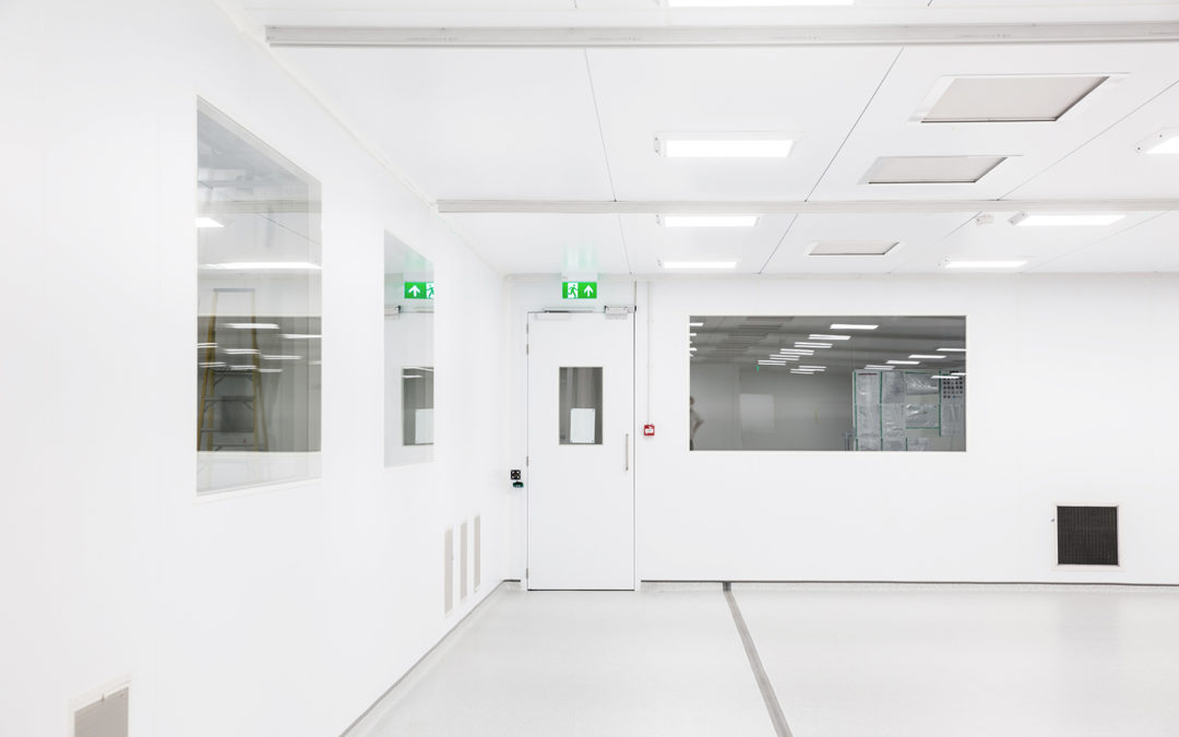
Since chips are highly susceptible to damage, even the smallest particle could cause a defect. This is why the specification for semiconductor chip fabrication cleanrooms typically ranges from ISO class 4 to 6. A HardWall cleanroom would be able to achieve this level of particulate control for a pilot plant. Zones can provide segregated spaces with control of environmental parameters—such as temperature, humidity, and UV—to be optimized for various steps of the production process.
The packaging, assembly, and testing of circuits or chips could be performed in ISO class 7 or ISO class 8 cleanrooms, with all considerations handled on a project-by-project basis. Equipment can be enclosed in a modular cleanroom, either RigidWall or SoftWall construction.
Over the years, Angstrom Technology has served the semiconductor industry with a wide range of cleanrooms. We’ve put together a simple guide to help you understand more about what type of cleanroom is suitable for your process.

Whether you are an existing semiconductor specialist or looking to diversify — the Angstrom Technology team can support your organization.
Contact Angstrom Technology to discuss your semiconductor cleanroom
Our cleanrooms are proudly made in America. We have the expertise to support organizations looking to build domestic capacity in line with the principles of the CHIPS program.
Are you thinking about investing in a semiconductor cleanroom? Request a semiconductor cleanroom quote today, or contact our team of experts for more information.
