
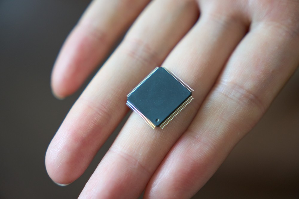
Semiconductor chips power nearly every modern technology, from smartphones and medical devices to advanced automotive systems, satellites, and defense equipment.
As chips become smaller, more complex, and increasingly critical to national supply chains, the environments in which they’re manufactured have also become more sophisticated.
That’s where semiconductor cleanrooms come in.
Semiconductor cleanrooms are controlled environments specifically engineered to protect highly sensitive wafers, prevent contamination, and support the ultra-precise processes required to manufacture semiconductor chips and today’s microelectronics.
Below, we break down what semiconductor cleanrooms are, why they matter, how they’re classified, and the design features needed to support safe, high-precision semiconductor production.
What Are Semiconductor Cleanrooms?
A semiconductor cleanroom is a controlled environment designed to maintain extremely low levels of airborne particles, temperature fluctuations, humidity variations, static, and molecular contamination.
These rooms are essential for wafer fabrication, lithography, etching, deposition, metrology, assembly, and packaging.
Even the tiniest particle — invisible to the human eye — can land on a wafer and ruin an entire batch of chips. Due to this, semiconductor cleanrooms must meet some of the most stringent ISO classifications in any industry.
Why Semiconductors Require Cleanroom Environments
Semiconductors are manufactured from ultra-pure silicon that’s melted, grown into a crystalline ingot, sliced into wafers, and processed through dozens to hundreds of steps to create micro-scale circuitry.
These wafers are extremely fragile. A single particle, static charge, or humidity shift can cause:
- Electrical defects
- Layer inconsistencies
- Reduced yield or complete batch loss
- Reliability issues in downstream devices
Because semiconductor performance has a direct impact on safety, defense, healthcare, transportation, and economic stability, cleanroom control is non-negotiable.
Industry News & Growth: How the CHIPS Act Has Accelerated Cleanroom Demand
The CHIPS and Science Act of 2022 injected over $52 billion into U.S. semiconductor research, fabrication, and workforce development. Since then, the industry has seen:
- Major fab expansions and new U.S. manufacturing campuses
- Increased investment in R&D and advanced packaging
- Rising demand for fast, modular, scalable cleanroom solutions
- Heightened compliance expectations for environmental control
Fab operators, OEMs, and R&D centers now require cleanrooms that can evolve quickly, support higher production capacity, and meet today’s ISO and industry-specific requirements.
If your organization is expanding semiconductor operations, planning a new fab, or upgrading existing facilities, cleanroom design is a critical first step.
Semiconductor Cleanroom Applications
Semiconductor cleanrooms are essential anywhere wafers or microelectronic components are processed. Common applications include:
- Wafer fabrication (front-end production)
- Lithography and photomask manufacturing
- Etching, deposition, and chemical processing
- Metrology, testing, and quality control
- Assembly, packaging, and dicing
- R&D, microelectronics prototyping, and advanced materials research
Industries that rely on semiconductor cleanrooms include:
- Consumer electronics
- Automotive & EV systems
- Aerospace & defense
- Robotics and automation
- Medical devices
- Household appliances
- Telecommunications and data centers
Any environment that requires precision, purity, and reliability necessitates a semiconductor-grade cleanroom.
Semiconductor Cleanroom Classifications (ISO Standards)
Most semiconductor manufacturing occurs in ISO 14644-1 Class 4–6 cleanrooms, particularly during wafer fabrication. These classes allow particle limits between:
- 352 – 35,200 particles/m³ at 0.5 μm
Less particle-sensitive steps, such as assembly, packaging, or testing, may use ISO Class 7 or Class 8.
In addition to ISO 14644-1, semiconductor cleanrooms must comply with:
- ISO 14644-2 (ongoing monitoring + quality control)
- ASTM standards for automotive semiconductor applications
- NASA environmental standards for aerospace microelectronics
- ESD and static control standards
Consistency is critical. A deviation in cleanliness, humidity, or static control can result in contamination, yield loss, or defective devices.
4 Key Semiconductor Cleanroom Design Features
Semiconductor cleanrooms require a highly engineered design that supports:
- Extreme precision
- Continuous operation
- High-volume airflow
- Personnel safety
- Static and humidity control
Below are the most critical elements:
1. ESD & Static Control
Electrostatic discharge (ESD) is one of the most damaging risks in semiconductor manufacturing. Cleanroom design must include:
- Static-dissipative flooring
- ESD-safe wall panels and furniture
- Proper grounding and bonded surfaces
- ESD garments and operator protocols
Without static control, a single discharge event can destroy circuitry.
2. Air Quality & Filtration
Semiconductor cleanrooms typically use:
- HEPA or ULPA filtration
- Laminar airflow systems to sweep particles downward
- Recirculating air plenums and air return walls
- Equipment-level exhaust for particle removal
Air changes per hour (ACH) are incredibly high in semiconductor settings, sometimes reaching hundreds of air exchanges per hour.
3. Humidity & Temperature Control
Moisture and thermal instability can cause:
- Wafer warping
- Adhesion failures
- Corrosion and surface swelling
- Solvent evaporation
Most semiconductor cleanrooms maintain a relative humidity of 35–45% with tight temperature control to preserve process accuracy.
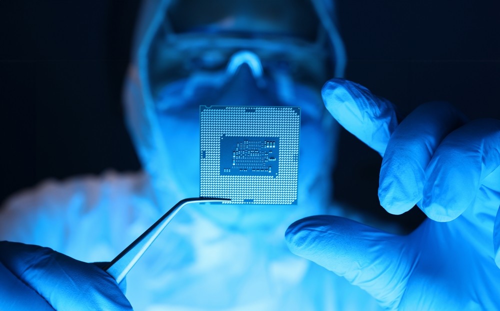
4. Operator Safety & Workflow
Operators are both a contamination risk and vulnerable to hazards in semiconductor manufacturing. Cleanroom design must support:
- Safe handling of hazardous gases, chemicals, and solvents
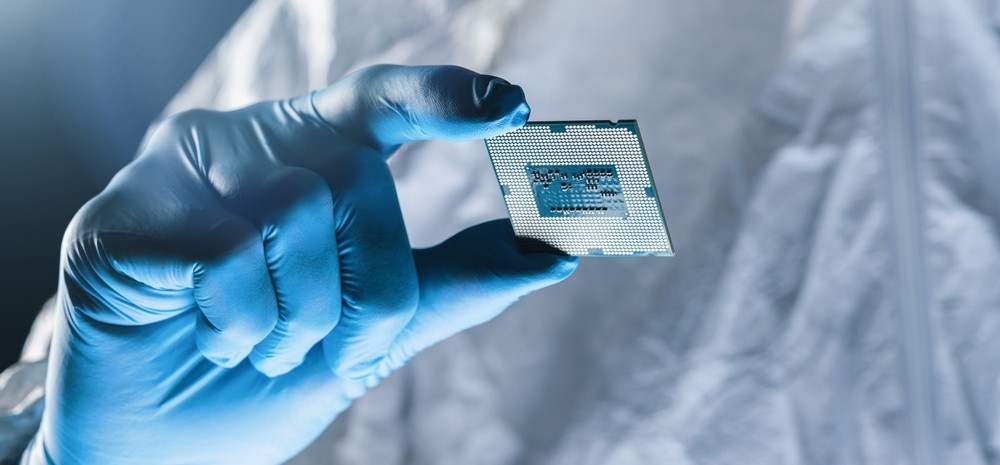
- Proper gowning procedures
- Segregated airflow zones
- Robotics or automated handling systems
- Laser and radiation safety considerations
Thoughtful layout reduces cross-contamination and improves throughput.
Considering a Semiconductor Cleanroom Project? Angstrom Can Help
As semiconductor manufacturing continues to expand rapidly across the U.S., many organizations are planning or upgrading their cleanroom environments to meet the new demands for output, precision, and compliance.
Angstrom Technology designs, engineers, and builds semiconductor cleanrooms that meet ISO standards, industry-specific requirements, and your facility’s unique environmental control needs.
Whether you’re expanding an existing fab or building a new R&D space, we deliver cleanrooms that support:
- High-volume production
- Ultra-clean air handling
- Robust ESD control
- Safe workflows for sensitive processes
- Scalable growth
Ready to bring your semiconductor cleanroom to life? Request a quote or speak with our cleanroom design experts today.
Semiconductor Cleanroom FAQs
Q. What is a semiconductor cleanroom?
A. A semiconductor cleanroom is a highly controlled environment designed to maintain extremely low levels of particles, static, humidity, and molecular contamination. These rooms are essential for wafer fabrication, lithography, etching, deposition, and other microelectronics processes where even microscopic particles can damage chips.
Q. Why do semiconductor chips need cleanrooms?
A. Semiconductor wafers are incredibly sensitive. Any particle, static charge, or humidity fluctuation can cause defects, reduce yield, or result in total batch loss. Cleanrooms ensure stable, contaminant-free conditions.
Q. What ISO class is required for semiconductor manufacturing?
A. Most semiconductor fabrication takes place in ISO Class 4–6 cleanrooms, which allow between 352 and 35,200 particles per cubic meter at 0.5 μm. Less sensitive processes, such as assembly, packaging, and testing, may occur in ISO Class 7 or 8 environments.
Q. How do semiconductor cleanrooms control contamination?
A. Contamination is controlled through:
- HEPA/ULPA filtration and laminar airflow
- High air-change rates
- ESD-dissipative flooring and surfaces
- Strict gowning protocols
- Humidity and temperature control
- Segregated process zones and equipment exhaust
Q. What special design features do semiconductor cleanrooms need?
A. Key design features include:
- Static control materials (floors, wall panels, furniture)
- Tight humidity and temperature control
- High-volume airflow with recirculating plenums
- Equipment-level fume exhaust
- Chemical handling safety systems
- Robotics integration for wafer handling
Q. How has the CHIPS Act impacted semiconductor cleanroom demand?
A. The CHIPS and Science Act released more than $52 billion in U.S. semiconductor funding, leading to new fabrication plants, expansions, and R&D facilities. As a result, the need for scalable, fast-to-deploy semiconductor cleanrooms has grown significantly.
Q. What materials are best for semiconductor cleanrooms?
A. Semiconductor cleanrooms commonly use:
- ESD-safe wall panels and flooring
- Non-shedding modular systems
- Stainless steel or coated aluminum furniture
- Chemical-resistant surfaces
Does Angstrom Technology build semiconductor cleanrooms?
Yes.
Angstrom designs, engineers, and builds semiconductor cleanrooms that meet ISO 14644 standards, ESD requirements, and specific environmental needs for each application. We support wafer fabrication, R&D labs, packaging facilities, and large-scale fab expansions.
Request a semiconductor cleanroom quote to get started.
